
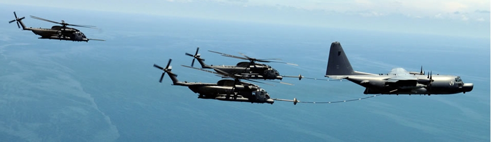
Our heavyweight helicopter equal in the world does not have
In Rostov started production of the most load-lifting rotary-wing car The Russian holding «Helicopt[...]

Everything about aircrafts and helicopters. News and events in aviation worldwide. Civil, transportation, military helicopters and airplanes.
Everything about aircrafts and helicopters. News and events in aviation worldwide. Civil, transportation, military helicopters and airplanes.
Everything about aircrafts and helicopters. News and events in aviation worldwide. Civil, transportation, military helicopters and airplanes.

Everything about aircrafts and helicopters. News and events in aviation worldwide. Civil, transportation, military helicopters and airplanes.


An internally gated CCD camera is promising for luminescent lifetime imaging. Fisher et al. (1999) developed a phase-sensitive CCD camera system for twodimensional imaging of concentrations of radical species in reacting flows such as turbulent flames. They modified a commercial scientific-grade CCD camera to perform phase-sensitive imaging as well as to reduce the level of integrated background light. In fact, this internally gated CCD camera has the capability to selectively integrate the time-varying luminescent intensity either in-phase or out – of-phase with respect to the modulated excitation light. A ratio between the out – of-phase and in-phase images is related to the luminescent lifetime, and thus a pressure field can be obtained from a luminescent lifetime image.
Modern CCD cameras available for industrial machine vision or scientific uses possess many of the features required to construct a phase-sensitive imaging system. Most notably, the feature commonly referred to as ‘electronic shuttering’ can be suitably modified to serve phase sensitive imaging or lifetime imaging. The CCD array architecture employed by cameras capable of performing electronic shuttering is referred to as an interline transfer array shown in Fig. 6.12. It consists of photodiodes separated by vertical transfer registers that are covered by an opaque metal shield that prevents direct entry of photoelectrons. Charge accumulated in the photosensors can be transferred either to the vertical registers or discarded in the substrate by supplying a high voltage to the Read Out Gate (ROG) or the Over Flow Drain (OFD) respectively.
In order to perform phase-sensitive imaging, charge shifting and storage in the CCD must be synchronized with the light-source modulation signal. This requires appropriate modification of the camera controller logic, and of the camera head circuitry and logic. Based on the modulation waveform, a suitable control signal will be generated, which raises the ROG voltage and lowers the OFD voltage during the in-phase half of the cycle. The in-phase luminescent signal is thus integrated into the vertical register. In the out-of-phase half of the modulation cycle, the ROG and OFD voltages are reversed, thus dumping the out-of-phase light into the substrate. This process is repeated for a number of cycles until the full-well capacity of the vertical registers is utilized to maximize the SNR. Finally, after the desired integration time (or the number of cycles) the accumulated charge in the vertical registers can be read out through the horizontal register using conventional frame transfer techniques. The out-of-phase image can be similarly obtained, the only difference being the introduction of a 180° phase lag between the modulation signal and the control signal described above. As pointed out before, a ratio between the out-of-phase and in-phase intensity images, I2 /Ij, is a function of the phase angle or the luminescent lifetime; therefore, a pressure field can be obtained from the luminescent lifetime image.
|
Fig. 6.12. Interline transfer CCD architecture and charge flow |


